Contents
Opamp input currents
An ideal opamp input would not draw any input current. In a precision DC
application, the effect of input currents flowing through a source
resistance must be included in the error budget.
The values listed for the non-inverting input bias current are the typical values at 25
degrees C. This parameter is used in preference to either the
maximum bias current at 25 deg C or the maximum bias current over
temperature because it is quoted for nearly all devices. Not all
applications are subjected to a wide temperature range.
The behaviour of the bias current depends on the opamp input circuitry.
If bias current is important in your circuit, you will need to understand the behaviour of the different types of input circuit.
JFET inputs
Opamps with FET inputs will have small input currents which are just
leakage currents. The input currents may be positive or negative, and
can have different polarities on the two inputs. FET gate leakage
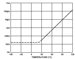
currents also typically double with every 10 degree rise in chip
temperature. This graph shows how the bias current varies with temperature for a typical device.

This graph suggests that very low bias currents can be achieved. An
important caveat is that the inputs must be operating within all the
manufacturer's limits, which will almost certainly include limits on
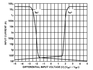
common mode voltages and differential mode voltages. The next graph
shows how protection diodes kick in when the differential voltage
becomes too large.

This limit on differential voltage should not become a problem during
normal operation because the differential input voltage is normally
negligible when the loop is closed.
Bipolar inputs
Bipolar transistors require a significant bias current of a predictable
polarity. NPN transistors require positive current to flow in to the
base, and PNP transistors require negative current to flow out of the
base. The polarity of the input bias current is important when
polarised capacitors are used to create some form of AC
filtering, as is common in audio applications. Although the base
currents can be reduced at will, the tradeoff is an inevitable increase
in noise and decrease in speed. As the bias currents for the two inputs
are approximately equal, their effect can be cancelled out if the
circuit uses matched bias resistors. In this case, only the difference
in bias currents will contribute to circuit errors. This difference in
bias currents is the "Input offset current", and may be specified by
the device manufacturer.
Some device contain additional current sources to provide the requisite input current.


